
Mechanical dicing can be done in a variety of ways. Wax or specialty tape are used to stabilize the wafer while the process is running. Both approaches can help avoid bottom-side chipping, but they take time and are labor-intensive. Mechanical dicing is best suited to individuals who can do the task without the need of specialist equipment. The most prevalent approaches are listed below. Continue reading to find out more. Wafer scribing, also known as mechanical dicing, is an industrial procedure for cutting semiconductor wafers into microscopic pieces.
Wafer scribing
Dicing is the mechanical separation of individual dies from a wafer. This process is often utilized for thin wafers that are less than 10 mils thick. Sawing is recommended when wafers are thicker. Following the dicing stage, the break step separates the wafer into individual dice. Dicing can be done in two or more processes, depending on the pattern.
Because the tool tip is small, it’s impossible to discern the exact location of the cutting point throughout the scribing operation. Furthermore, considerable testing is required to guarantee that the cuts are exact and within specification. The old method took a long time and was highly reliant on the operator’s ability. The new technology, on the other hand, can eliminate many of the drawbacks of manual dicing while also reducing dicing time and cost.
Wafer breaking
Mechanical dicing is widely utilized in semiconductor production, with faster throughput and precision becoming more important. Productivity and yield are determined by the rate at which wafer substrates are fed into the cutting blade. Blade yield and chipping are two important restrictions that must be closely monitored. To establish the maximum feed rate without exceeding the limits, a unique monitoring mechanism is necessary. The torque supplied to the cutting blade is monitored by this parameter.
With a claimed throughput of 12 wafers per hour for JPSA, the rate of scribe & break die singulation is the greatest in a thin scribe. Although GaAs scribing is significantly quicker, actual rates are dependent on the crystal type, alignment, and dicing lanes employed. Partially scribe cuts are performed along the wafer’s cleavage plane using a laser or mechanical saw, resulting in a crack for the break.
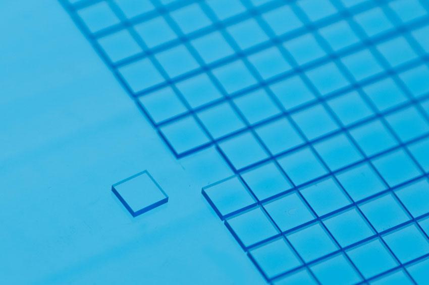
Wafer dicing tape
Dicing is a crucial step in the semiconductor manufacturing process. The wafers are attached on a sticky back piece of tape and mechanically sliced by pressing the tape against a thin metal frame in this method. Dicing tapes come in a variety of thicknesses and qualities, and they’re utilized for a variety of purposes. One variety, for example, is UV curable, whereas the other is not. Small and big dies are made using both types of tapes. Die streets are created when the dies are sliced, and the pieces are generally 75 micrometers (0.003 inch) broad.
A pressure-sensitive adhesive or release film covers a base plastic film on a traditional dicing tape. For mechanical dicing, it is used to cover the edge of a silicon wafer. It’s generally blue in hue and comes at a reasonable cost. Some dicing tapes may be utilized with regular silicon wafers since they are UV-released. ESD tape is another type of dicing tape that is used to safeguard semiconductor dies.
Etching
A semiconductor wafer is thinned to a specific depth and then mounted to a taped dicing frame in a process that combines etching and mechanical dicing. Etching is used to construct roadways all the way down to the tape. When compared to mechanically diced wafers, the notching at the interface weakens the die in this method. Depending on the intended dicing patterns, etching processes can be used in a variety of ways.
One method involves using specialized tape and wax to stabilize the wafer as it is being diced. This approach can prevent chipping on the bottom surface, however it is time consuming and sluggish. The dies are then taped to the dicing tape and left there until they are removed. The drawback of this process is that it is more labor-intensive, which might slow down output. In other circumstances, though, the advantages exceed the disadvantages.
Plasma dicing
Dicing has been a popular solution for semiconductor makers as dies get thinner and smaller. The plasma dicing enables accurate, non-contact mechanical dicing of thin silicon wafers, which is particularly useful for devices with small, fine features. Dicing may be used to dice wafers without destroying them since it does not require a straight dicing route.
Dicing, in addition to its etching capabilities, has a number of benefits over previous approaches. First, it chemically eliminates material with no heat-affected zones. Plasma dicing has a stronger break strength than laser or blade dicing, and it can keep dies that are subjected to severe physical pressures mechanically intact. Hybrid bonding stacks, such as high-bandwidth memory, benefit greatly from this approach.